
 EN
EN
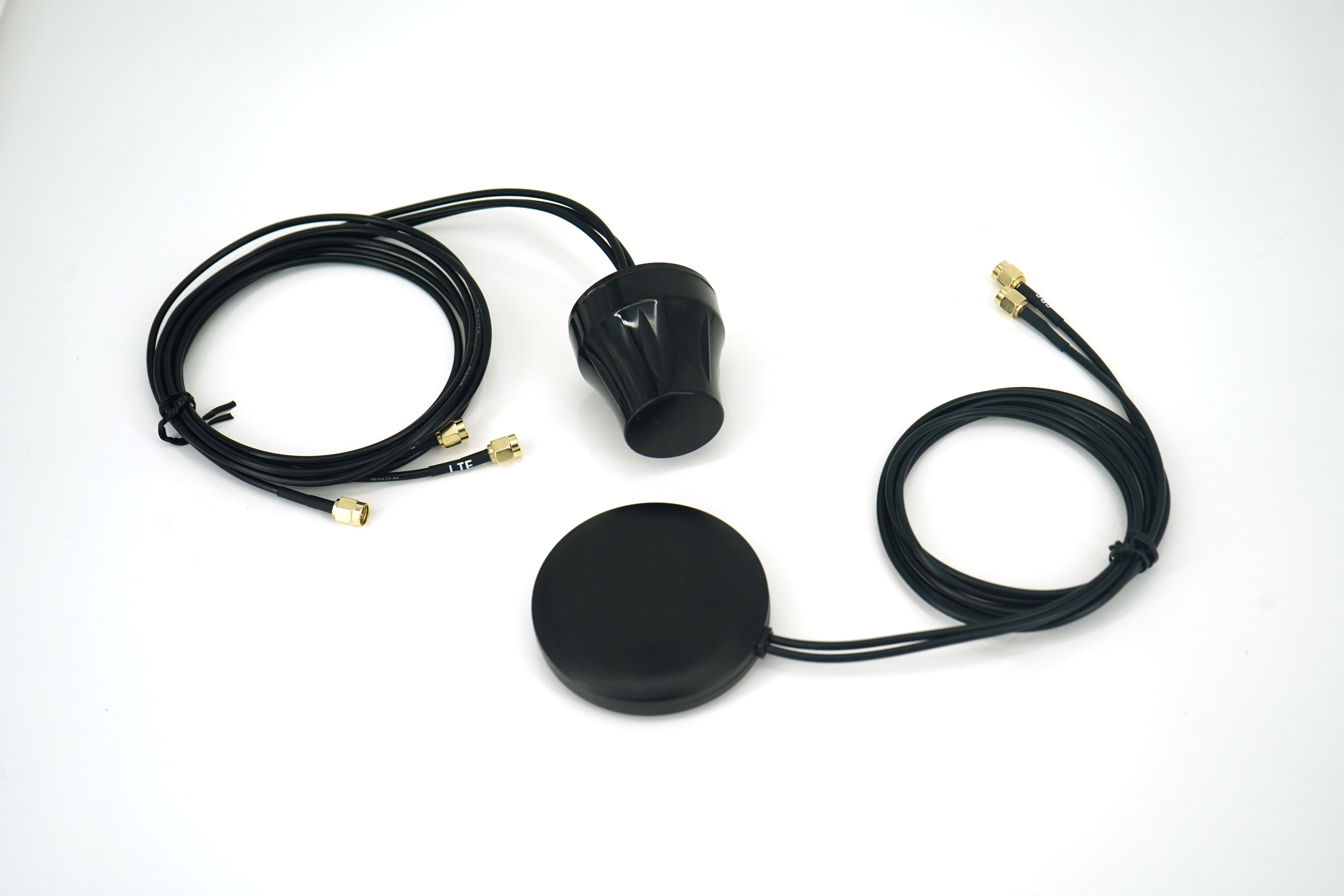
Modern wireless communication systems demand antennas that combine exceptional performance with compact form factors, leading to the widespread adoption of ceramic patch antenna technology. These innovative components have revolutionized the telecommunications industry by offering superior electrical properties, thermal stability, and miniaturization capabilities that traditional antenna materials cannot match. As we advance into 2025, the ceramic patch antenna continues to set new standards for efficiency and reliability in demanding applications ranging from satellite communications to 5G networks.

The unique properties of ceramic materials make them ideal substrates for patch antenna construction, offering high dielectric constants that enable significant size reduction without compromising performance. Engineers worldwide rely on ceramic patch antenna solutions to meet increasingly stringent requirements for bandwidth, gain, and power handling in space-constrained environments. This comprehensive guide explores the fundamental principles, design considerations, and best practices that define successful ceramic patch antenna implementation in contemporary wireless systems.
Understanding Ceramic Patch Antenna Fundamentals
Core Material Properties and Advantages
The foundation of any effective ceramic patch antenna lies in the exceptional properties of ceramic dielectric materials. These substrates typically exhibit dielectric constants ranging from 6 to 100, significantly higher than conventional materials like FR4 or Rogers substrates. This high permittivity enables dramatic size reduction, with ceramic patch antenna elements often 70-90% smaller than their conventional counterparts while maintaining equivalent electrical performance.
Temperature stability represents another critical advantage of ceramic patch antenna technology. Premium ceramic materials demonstrate temperature coefficients of resonant frequency as low as ±10 ppm/°C, ensuring consistent performance across wide operating temperature ranges. This stability proves essential in aerospace, automotive, and industrial applications where environmental conditions vary significantly. Additionally, ceramic substrates offer excellent mechanical durability, withstanding shock, vibration, and thermal cycling that would damage traditional antenna materials.
Electromagnetic Characteristics and Performance Metrics
The electromagnetic behavior of a ceramic patch antenna differs substantially from conventional designs due to the unique field distribution patterns created by high-permittivity substrates. The concentrated electromagnetic fields within the ceramic material result in improved radiation efficiency and reduced spurious emissions. Quality factors typically exceed 1000 in well-designed ceramic patch antenna systems, contributing to excellent selectivity and minimal insertion loss.
Bandwidth characteristics of ceramic patch antenna designs require careful consideration during the design phase. While the high dielectric constant enables miniaturization, it can also narrow the operational bandwidth compared to lower-permittivity alternatives. Modern design techniques, including stacked configurations and aperture coupling, help overcome these limitations while preserving the size advantages that make ceramic patch antenna technology so valuable in compact applications.
Design Methodology and Engineering Considerations
Dimensional Scaling and Resonance Calculations
Proper dimensional scaling forms the cornerstone of successful ceramic patch antenna design. The effective length and width calculations must account for the complex field distributions that occur at the interface between the ceramic substrate and surrounding air. Standard patch antenna formulas require modification factors that consider the high dielectric contrast and the resulting field concentration effects unique to ceramic implementations.
Resonance frequency calculations for ceramic patch antenna designs involve sophisticated electromagnetic modeling to predict actual performance accurately. The effective dielectric constant experienced by the radiating fields differs from the bulk material properties due to fringing effects at the patch edges. Modern simulation tools incorporate these effects, enabling precise frequency targeting while accounting for the manufacturing tolerances inherent in ceramic processing techniques.
Feed Network Integration and Impedance Matching
Feed network design represents a critical aspect of ceramic patch antenna implementation, as the high dielectric constant environment affects impedance transformation and power distribution. Probe feeding remains popular for single-element designs, though careful attention to probe positioning and substrate thickness prevents unwanted resonances and maintains clean radiation patterns. The ceramic patch antenna technology offers multiple feeding options, each with specific advantages for different applications.
Aperture coupling techniques provide excellent isolation between feed networks and radiating elements in ceramic patch antenna arrays. This approach proves particularly valuable in phased array applications where mutual coupling between elements must be minimized. The ceramic substrate's properties enable compact aperture designs that maintain excellent bandwidth and efficiency characteristics while supporting complex beamforming requirements.
Manufacturing Processes and Quality Control
Ceramic Substrate Preparation and Processing
The manufacturing process for ceramic patch antenna substrates begins with careful material selection and formulation. High-purity ceramic powders undergo precise mixing and pressing procedures to achieve the desired dielectric properties and mechanical characteristics. Sintering temperatures and atmospheric conditions require strict control to prevent variations that could affect electrical performance or introduce unwanted losses in the finished ceramic patch antenna assembly.
Surface preparation and metallization processes significantly impact the final performance of ceramic patch antenna products. Clean room environments prevent contamination that could degrade electrical properties or introduce reliability issues. Advanced deposition techniques, including sputtering and electroplating, create uniform conductor layers with excellent adhesion to the ceramic substrate, ensuring long-term stability and consistent performance across production batches.
Pattern Definition and Precision Etching
Pattern definition for ceramic patch antenna elements demands exceptional precision to achieve specified electrical characteristics. Photolithographic processes adapted for ceramic substrates enable feature sizes below 50 micrometers while maintaining excellent edge definition and dimensional accuracy. The etching chemistry and process parameters require optimization for ceramic materials to prevent undercutting or surface roughening that could degrade antenna performance.
Quality control throughout the ceramic patch antenna manufacturing process involves comprehensive electrical and mechanical testing. Automated test equipment verifies resonance frequency, return loss, radiation patterns, and gain characteristics against design specifications. Statistical process control techniques identify trends and variations that might indicate process drift, enabling corrective action before defective products reach customers.
Performance Optimization Strategies
Bandwidth Enhancement Techniques
Bandwidth optimization in ceramic patch antenna designs requires innovative approaches that leverage the unique properties of ceramic substrates while addressing their inherent limitations. Stacked patch configurations utilize multiple resonant elements at slightly different frequencies to broaden the overall bandwidth. The high dielectric constant of ceramic materials enables compact stacked designs that would be impractical with conventional substrates.
Parasitic element coupling represents another effective bandwidth enhancement strategy for ceramic patch antenna systems. Carefully positioned parasitic patches create additional resonances that merge with the primary element's response, extending usable bandwidth while maintaining acceptable VSWR characteristics. The precise control possible with ceramic fabrication processes enables optimal parasitic element positioning that maximizes bandwidth improvement.
Efficiency Improvement and Loss Minimization
Maximizing radiation efficiency in ceramic patch antenna designs requires attention to multiple loss mechanisms that can degrade performance. Conductor losses become particularly significant in miniaturized designs where current densities increase due to reduced conductor dimensions. High-conductivity metallization systems, including gold and silver-based conductors, minimize these losses while providing excellent environmental stability.
Dielectric losses within the ceramic substrate itself represent another important consideration for ceramic patch antenna optimization. Low-loss ceramic formulations, characterized by loss tangents below 0.001, preserve signal quality and maximize radiation efficiency. Surface wave suppression techniques, including textured ground planes and absorptive boundary conditions, prevent unwanted coupling between antenna elements in array configurations.
Application-Specific Design Guidelines
Satellite Communication Systems
Satellite communication applications impose unique requirements on ceramic patch antenna designs, including operation at multiple frequency bands and circular polarization capabilities. The compact size enabled by ceramic substrates proves invaluable in spacecraft applications where mass and volume constraints are critical. Thermal cycling requirements in space environments benefit from the excellent temperature stability of ceramic patch antenna technology.
Phased array implementations for satellite communications utilize ceramic patch antenna elements to achieve precise beam steering and null placement. The consistent electrical properties across ceramic substrates enable accurate amplitude and phase control essential for adaptive beamforming algorithms. Integration with solid-state power amplifiers becomes more straightforward due to the thermal management capabilities inherent in ceramic designs.
5G and Beyond Wireless Networks
The deployment of 5G networks and emerging 6G technologies creates unprecedented demands for ceramic patch antenna solutions that support millimeter-wave frequencies and massive MIMO implementations. The size reduction capabilities of ceramic substrates enable practical antenna arrays with hundreds or thousands of elements within manageable form factors. Beam steering accuracy and side lobe suppression benefit from the dimensional stability and uniform properties of ceramic patch antenna assemblies.
Integration with advanced semiconductor technologies, including GaN and SiGe components, requires ceramic patch antenna designs optimized for high power density and thermal management. The thermal conductivity of ceramic substrates helps distribute heat generated by active components while maintaining electrical isolation. Multi-band operation capabilities enable ceramic patch antenna systems to support diverse 5G frequency allocations while minimizing system complexity.
Future Trends and Emerging Technologies
Advanced Material Development
Research into next-generation ceramic materials continues to push the boundaries of ceramic patch antenna performance. Low-temperature co-fired ceramic (LTCC) technologies enable integration of passive components and embedded conductors within the antenna substrate, reducing assembly complexity and improving electrical performance. These advances promise even more compact ceramic patch antenna solutions with enhanced functionality.
Metamaterial-inspired ceramic compositions offer the possibility of engineered electromagnetic properties that optimize ceramic patch antenna performance for specific applications. Negative refractive index materials and artificial magnetic conductors fabricated using ceramic processes could enable unprecedented miniaturization and bandwidth capabilities in future ceramic patch antenna designs.
Manufacturing Innovation and Automation
Additive manufacturing techniques adapted for ceramic materials present opportunities for rapid prototyping and customization of ceramic patch antenna designs. Three-dimensional printing of ceramic substrates with integrated conductors could revolutionize the manufacturing process while enabling complex geometries impossible with traditional fabrication methods. Quality control systems incorporating machine learning algorithms will optimize ceramic patch antenna production processes and predict performance characteristics.
Automated assembly and testing systems specifically designed for ceramic patch antenna production will improve consistency and reduce manufacturing costs. Integration with enterprise resource planning systems will enable real-time optimization of production parameters based on performance feedback and yield data. These advances will make ceramic patch antenna technology accessible for a broader range of applications and market segments.
FAQ
What are the main advantages of ceramic patch antenna technology over conventional designs
Ceramic patch antenna technology offers several significant advantages including dramatic size reduction due to high dielectric constants, excellent temperature stability with coefficients as low as ±10 ppm/°C, superior mechanical durability for harsh environments, and improved radiation efficiency through concentrated electromagnetic fields. These benefits make ceramic patch antennas ideal for space-constrained applications requiring reliable performance across wide temperature ranges.
How does the high dielectric constant of ceramic materials affect antenna bandwidth
The high dielectric constant in ceramic patch antenna designs typically results in narrower bandwidth compared to lower-permittivity alternatives due to increased quality factor and field concentration effects. However, modern design techniques including stacked configurations, parasitic element coupling, and aperture coupling can effectively broaden bandwidth while preserving the miniaturization benefits of ceramic substrates.
What manufacturing considerations are critical for ceramic patch antenna production
Critical manufacturing considerations include precise control of ceramic sintering temperatures and atmospheres to maintain consistent dielectric properties, clean room environments to prevent contamination, advanced metallization processes for uniform conductor layers, high-precision photolithography for accurate pattern definition, and comprehensive quality control testing throughout production to ensure electrical and mechanical specifications are met.
Which applications benefit most from ceramic patch antenna technology
Applications that benefit most from ceramic patch antenna technology include satellite communications requiring compact, temperature-stable designs, 5G and millimeter-wave systems needing miniaturized array elements, aerospace applications where mass and volume constraints are critical, automotive systems exposed to harsh environmental conditions, and IoT devices requiring small form factors with reliable wireless connectivity. The technology is particularly valuable where traditional antenna designs cannot meet size or performance requirements.
Table of Contents
- Understanding Ceramic Patch Antenna Fundamentals
- Design Methodology and Engineering Considerations
- Manufacturing Processes and Quality Control
- Performance Optimization Strategies
- Application-Specific Design Guidelines
- Future Trends and Emerging Technologies
-
FAQ
- What are the main advantages of ceramic patch antenna technology over conventional designs
- How does the high dielectric constant of ceramic materials affect antenna bandwidth
- What manufacturing considerations are critical for ceramic patch antenna production
- Which applications benefit most from ceramic patch antenna technology