
 EN
EN
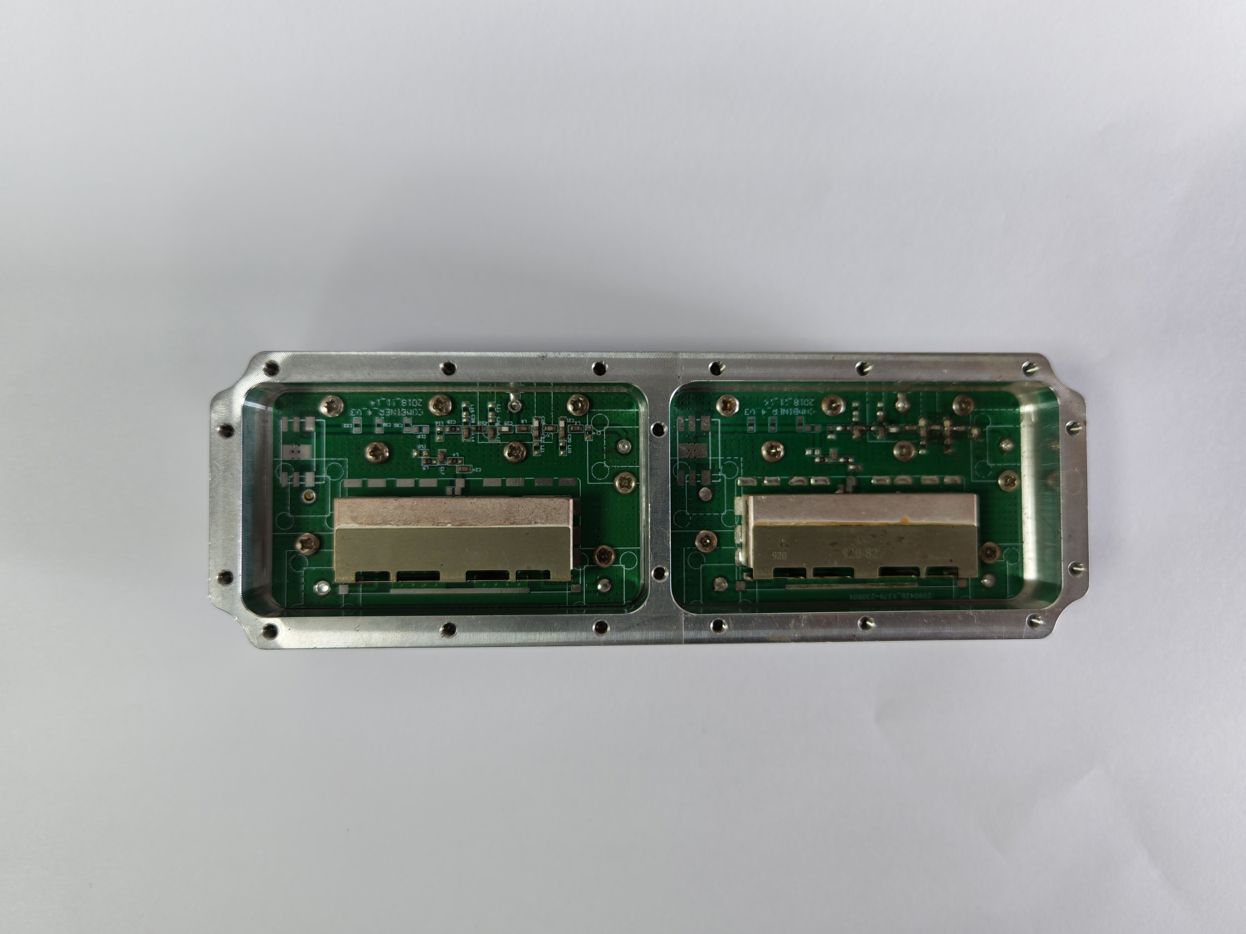
Modern wireless communication systems demand increasingly sophisticated antenna solutions that balance performance, size, and manufacturing efficiency. Engineers face critical decisions when selecting between ceramic patch antenna designs and traditional printed circuit board implementations. This comprehensive analysis explores the fundamental differences, performance characteristics, and economic considerations that influence antenna selection in contemporary RF applications. Understanding these distinctions enables informed decision-making for applications ranging from IoT devices to high-frequency communication systems.

Fundamental Design Principles and Material Properties
Ceramic Substrate Characteristics
The ceramic patch antenna leverages high-dielectric-constant ceramic materials that fundamentally alter electromagnetic wave propagation characteristics. These materials typically exhibit dielectric constants ranging from 10 to 100, significantly higher than conventional PCB substrates. The elevated dielectric constant enables substantial size reduction while maintaining operational frequency characteristics. Ceramic materials demonstrate exceptional thermal stability, maintaining consistent electrical properties across wide temperature ranges that would compromise PCB-based designs.
Temperature coefficient specifications for ceramic materials often achieve stability within ±15 ppm/°C, compared to PCB substrates that may experience variations exceeding ±100 ppm/°C. This thermal stability directly translates to frequency stability in practical applications. Ceramic substrates also exhibit superior mechanical durability, resisting deformation and maintaining dimensional accuracy under physical stress conditions that would permanently damage PCB structures.
PCB Substrate Properties
Traditional PCB antenna implementations utilize fiberglass-epoxy composites with dielectric constants typically ranging from 3.5 to 10. While these materials offer lower dielectric constants compared to ceramics, they provide advantages in manufacturing flexibility and design modification capabilities. PCB substrates enable rapid prototyping and iterative design optimization through standard fabrication processes familiar to most electronics manufacturers.
The ceramic patch antenna design constrains modification opportunities once manufacturing begins, while PCB implementations support design changes through standard etching and drilling procedures. PCB materials also demonstrate predictable aging characteristics, with well-documented performance degradation patterns that facilitate long-term reliability planning. However, PCB substrates exhibit greater susceptibility to moisture absorption, potentially affecting electrical characteristics in humid environments.
Performance Analysis and Efficiency Metrics
Frequency Response Characteristics
Performance evaluation reveals distinct frequency response patterns between ceramic patch antenna and PCB implementations. Ceramic designs typically achieve broader bandwidth characteristics due to the substrate's intrinsic properties and reduced conductor losses. The high dielectric constant of ceramic materials enables resonant frequency reduction while maintaining compact physical dimensions, particularly advantageous for space-constrained applications.
Measurement data consistently demonstrates that ceramic patch antenna designs achieve return loss performance exceeding -25 dB across operational bandwidths, compared to typical PCB implementations that achieve -15 dB to -20 dB performance. The superior return loss performance directly correlates to improved power transfer efficiency and reduced signal reflection. Ceramic implementations also exhibit more stable frequency response characteristics across temperature variations, maintaining consistent performance in demanding environmental conditions.
Radiation Pattern and Gain Performance
Radiation pattern analysis reveals fundamental differences in electromagnetic field distribution between ceramic and PCB antenna designs. The ceramic patch antenna generates more uniform radiation patterns with reduced back-lobe radiation compared to PCB equivalents. This characteristic stems from the ceramic substrate's ability to better contain electromagnetic fields, reducing spurious radiation and improving overall antenna efficiency.
Gain measurements typically favor ceramic implementations, with realized gain improvements of 2-3 dB common across frequency ranges. The improved gain performance results from reduced dielectric losses and better field confinement within the ceramic substrate. Additionally, ceramic designs demonstrate superior cross-polarization rejection, often achieving isolation levels exceeding 20 dB compared to PCB designs that typically achieve 15 dB isolation.
Manufacturing Considerations and Production Scalability
Fabrication Process Requirements
Manufacturing processes for ceramic patch antenna production require specialized equipment and controlled environmental conditions not typically required for PCB fabrication. Ceramic processing involves high-temperature sintering operations, often exceeding 1200°C, demanding specialized furnaces and precise temperature control systems. These requirements significantly impact initial capital investment and ongoing operational costs for manufacturers.
Quality control procedures for ceramic antenna production necessitate advanced measurement capabilities and statistical process control methodologies. Each ceramic patch antenna requires individual testing to verify performance specifications, while PCB designs often permit batch testing procedures. The specialized nature of ceramic processing also limits the number of qualified suppliers, potentially creating supply chain dependencies that don't exist for PCB-based designs.
Volume Production Capabilities
Production scalability differs substantially between ceramic and PCB antenna technologies. PCB manufacturing leverages established global infrastructure with numerous qualified suppliers and standardized processes. This infrastructure supports rapid volume scaling and competitive pricing for large-quantity orders. Standard PCB fabrication equipment can produce thousands of antenna elements simultaneously through panelization techniques.
Ceramic production typically requires individual piece processing, limiting throughput and increasing per-unit handling costs. However, the ceramic patch antenna manufacturing process eliminates many assembly steps required for PCB implementations, potentially offsetting some throughput limitations. Ceramic designs integrate the radiating element and substrate in a single component, reducing assembly complexity and improving long-term reliability.
Cost Structure Analysis and Economic Considerations
Initial Development and Tooling Costs
Development cost structures reveal significant differences between ceramic patch antenna and PCB approaches. Ceramic designs require substantial initial investment in material characterization, mold development, and process optimization. These upfront costs often exceed PCB development expenses by factors of 3-5, primarily due to the specialized nature of ceramic processing and limited supplier base.
However, ceramic designs often require fewer design iterations due to more predictable material properties and performance characteristics. PCB designs may require multiple prototype cycles to optimize performance, particularly for demanding applications. The ceramic development process also eliminates many variables associated with PCB fabrication, such as copper adhesion, via reliability, and substrate warpage concerns.
Production Volume Economics
Economic analysis must consider production volume thresholds where ceramic patch antenna solutions become cost-competitive with PCB alternatives. Low-volume applications typically favor PCB implementations due to lower setup costs and broader supplier availability. Break-even analysis often identifies volume thresholds between 10,000 and 100,000 units where ceramic solutions achieve cost parity.
High-volume production scenarios increasingly favor ceramic implementations due to reduced assembly costs and improved yield rates. Ceramic designs eliminate multiple assembly steps, reducing labor costs and potential failure points. Long-term cost projections must also consider material price stability, with ceramic materials demonstrating less price volatility compared to PCB substrates that fluctuate with copper and fiberglass market conditions.
Application-Specific Performance Requirements
Mobile and IoT Device Integration
Mobile device applications present unique requirements that influence antenna selection criteria. The ceramic patch antenna offers significant advantages in space-constrained environments, achieving comparable performance in substantially smaller form factors. Modern smartphones and IoT devices benefit from the size reduction potential of ceramic designs, enabling more compact product architectures.
Battery life considerations also favor ceramic implementations due to improved antenna efficiency and reduced power consumption. The superior performance characteristics of ceramic designs translate directly to extended battery operation in battery-powered devices. Additionally, ceramic materials demonstrate excellent compatibility with modern manufacturing processes used in mobile device production, including surface-mount technology and automated assembly systems.
Industrial and Automotive Applications
Industrial environments demand antenna solutions that maintain performance under extreme conditions including temperature cycling, vibration, and chemical exposure. Ceramic patch antenna designs excel in these demanding applications due to superior environmental stability and mechanical durability. Automotive applications particularly benefit from ceramic thermal stability, maintaining consistent performance across the -40°C to +125°C temperature range typical in automotive environments.
Long-term reliability requirements in industrial applications often justify the higher initial cost of ceramic solutions through reduced maintenance and replacement expenses. Ceramic designs demonstrate minimal performance degradation over operational lifetimes exceeding 20 years, while PCB implementations may require replacement or recalibration within 10-15 year timeframes due to material aging and environmental effects.
Future Technology Trends and Market Evolution
Emerging Material Technologies
Advanced ceramic formulations continue expanding the performance envelope for ceramic patch antenna applications. Low-temperature co-fired ceramic (LTCC) technology enables integration of passive components and routing within the ceramic substrate, creating truly integrated antenna modules. These advances blur traditional distinctions between ceramic and PCB approaches, offering hybrid solutions that combine benefits of both technologies.
Research into metamaterial-enhanced ceramic substrates promises further performance improvements and novel functionality. These advanced materials may enable beam-steering capabilities and adaptive frequency response within ceramic patch antenna designs. Simultaneously, PCB technology evolution includes development of high-frequency laminates and embedded component technologies that improve traditional PCB antenna performance.
Manufacturing Technology Advancement
Additive manufacturing techniques show promise for ceramic antenna production, potentially reducing tooling costs and enabling rapid prototyping of ceramic designs. Three-dimensional printing of ceramic materials with controlled dielectric properties may revolutionize ceramic patch antenna development processes. These manufacturing advances could significantly reduce the cost disadvantage traditionally associated with ceramic implementations.
Automation improvements in ceramic processing also promise reduced production costs and improved quality consistency. Advanced process control systems and artificial intelligence applications in ceramic manufacturing may achieve the production efficiency levels currently associated with PCB fabrication. These technological developments suggest converging cost structures between ceramic and PCB antenna solutions in future market conditions.
FAQ
What are the primary advantages of ceramic patch antenna designs over PCB implementations?
Ceramic patch antenna designs offer several key advantages including significantly smaller form factors due to high dielectric constants, superior thermal stability across wide temperature ranges, improved mechanical durability, better frequency stability, and enhanced radiation efficiency. These characteristics make ceramic designs particularly suitable for space-constrained applications and demanding environmental conditions where consistent performance is critical.
How do manufacturing costs compare between ceramic and PCB antenna solutions?
Initial development and low-volume production typically favor PCB solutions due to lower setup costs and broader supplier availability. However, ceramic patch antenna solutions often become cost-competitive at production volumes exceeding 10,000-100,000 units due to reduced assembly requirements and improved yield rates. Long-term total cost of ownership may favor ceramic solutions in applications requiring high reliability and minimal maintenance.
What performance differences should engineers expect between these technologies?
Engineers can expect ceramic patch antenna designs to deliver 2-3 dB improved gain performance, superior return loss characteristics often exceeding -25 dB, more uniform radiation patterns with reduced back-lobe radiation, and better cross-polarization rejection. Ceramic designs also maintain more stable performance across temperature variations and demonstrate superior bandwidth characteristics compared to equivalent PCB implementations.
Which applications benefit most from ceramic patch antenna technology?
Applications that benefit most from ceramic patch antenna technology include mobile devices requiring compact antenna solutions, IoT devices prioritizing battery life and size constraints, automotive systems demanding wide temperature range operation, industrial equipment requiring long-term reliability, and high-frequency communication systems where superior electrical performance justifies higher initial costs. Space-constrained and environmentally demanding applications particularly favor ceramic implementations.
Table of Contents
- Fundamental Design Principles and Material Properties
- Performance Analysis and Efficiency Metrics
- Manufacturing Considerations and Production Scalability
- Cost Structure Analysis and Economic Considerations
- Application-Specific Performance Requirements
- Future Technology Trends and Market Evolution
-
FAQ
- What are the primary advantages of ceramic patch antenna designs over PCB implementations?
- How do manufacturing costs compare between ceramic and PCB antenna solutions?
- What performance differences should engineers expect between these technologies?
- Which applications benefit most from ceramic patch antenna technology?