
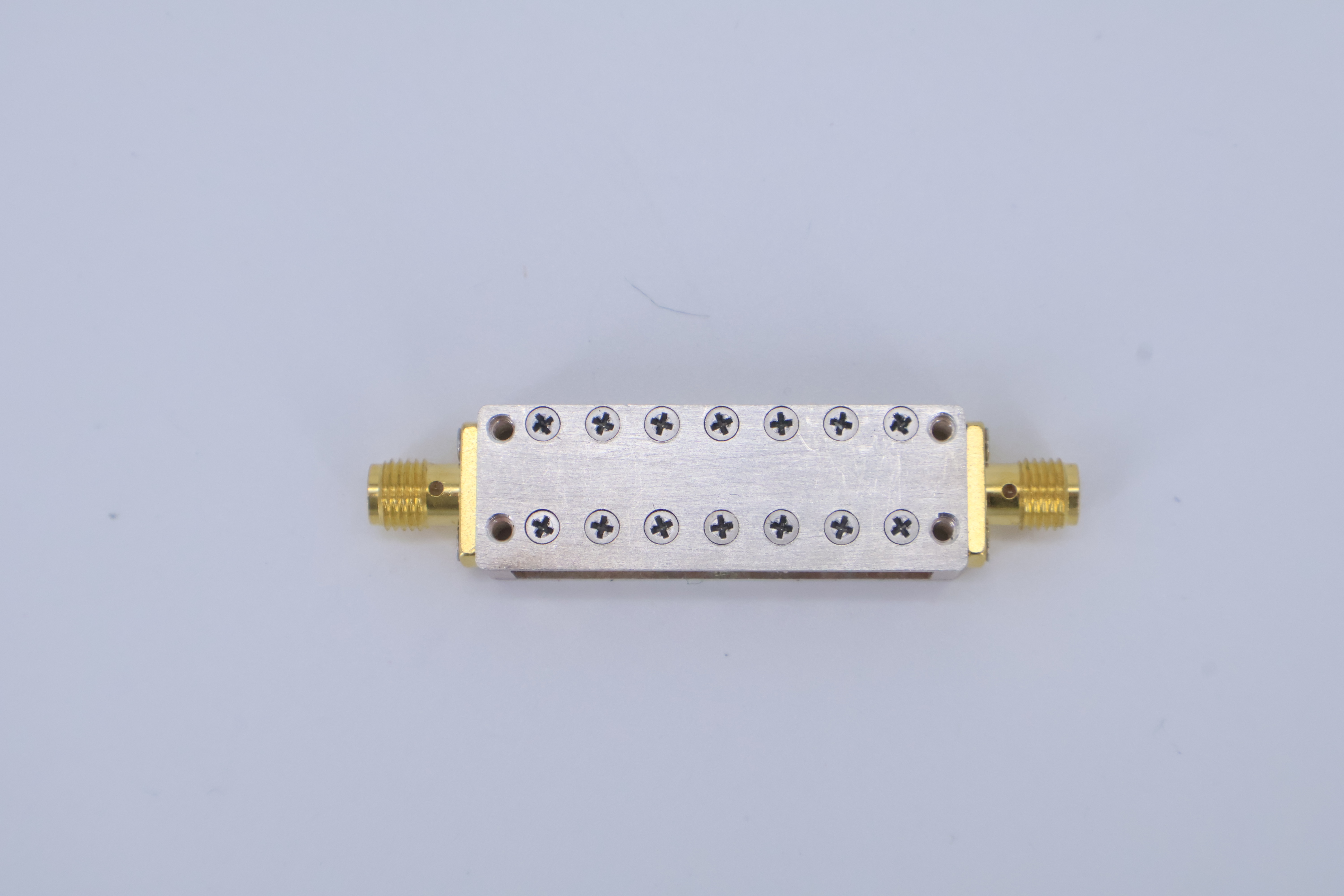
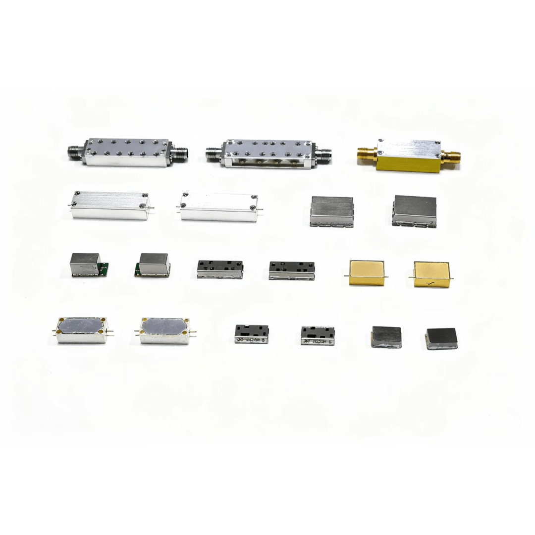
In radio frequency applications, achieving precise signal control requires sophisticated filtering techniques that can effectively eliminate unwanted frequency components while preserving desired signals. The lc band-stop filter represents one of the most fundamental yet powerful solutions for RF engineers seeking to attenuate specific frequency ranges in their circuit designs. These passive filters combine inductors and capacitors in strategic configurations to create notch characteristics that reject targeted frequencies with remarkable precision. Understanding the principles and implementation strategies of lc band-stop filter circuits becomes essential for anyone working with RF systems, from amateur radio enthusiasts to professional telecommunications engineers.
Fundamental Principles of LC Band-Stop Filter Design
Basic Circuit Topology and Component Interaction
The foundation of every lc band-stop filter lies in the resonant behavior of inductors and capacitors working in parallel configuration. When these reactive components are connected in parallel and placed in series with the signal path, they create a resonant circuit that presents minimum impedance at the resonant frequency. This low impedance effectively short-circuits the signal at the target frequency, causing maximum attenuation while allowing other frequencies to pass with minimal loss. The mathematical relationship governing this behavior follows the standard resonance formula, where the resonant frequency equals one divided by two pi times the square root of inductance multiplied by capacitance.
The quality factor of an lc band-stop filter determines both the sharpness of the notch and the insertion loss characteristics across the frequency spectrum. Higher quality factors result in narrower rejection bands with steeper roll-off rates, making them ideal for applications requiring surgical precision in frequency rejection. However, achieving high Q values often involves trade-offs in terms of component tolerances, temperature stability, and manufacturing costs. Professional RF designers must carefully balance these competing requirements to optimize filter performance for their specific applications.
Impedance Matching Considerations
Proper impedance matching plays a crucial role in maximizing the effectiveness of lc band-stop filter implementations. The filter must present the correct impedance to both source and load while maintaining its rejection characteristics across the desired frequency range. Mismatched impedances can lead to unwanted reflections, reduced attenuation depth, and unpredictable frequency response variations. Engineers typically employ network analysis techniques and Smith chart calculations to ensure optimal matching conditions throughout the operational bandwidth.
The characteristic impedance of the transmission line environment also influences filter design parameters significantly. Standard 50-ohm and 75-ohm systems require different component values and configuration adjustments to achieve identical frequency response characteristics. This impedance dependency necessitates careful consideration during the initial design phase to avoid costly redesign cycles and performance compromises in the final implementation.
Advanced Circuit Configurations for Enhanced Performance
Multiple Notch Filter Architectures
Complex RF applications often require rejection of multiple discrete frequencies or broader stopbands that exceed the capabilities of simple single-resonator lc band-stop filter designs. Multiple notch architectures employ cascaded resonant sections, each tuned to specific frequencies within the rejection band. This approach allows engineers to create custom stopband shapes with multiple attenuation peaks or extended rejection bandwidths while maintaining acceptable insertion loss in the passband regions.
The interaction between multiple resonant sections in cascaded lc band-stop filter configurations requires careful analysis to prevent unwanted coupling effects and frequency pulling phenomena. Proper isolation between stages through appropriate spacing and shielding techniques ensures that each resonator maintains its intended frequency response without interference from adjacent sections. Advanced simulation tools and electromagnetic modeling become essential for optimizing these complex multi-stage designs.
Broadband Rejection Techniques
When applications demand rejection of wide frequency bands rather than discrete notches, engineers can implement broadband lc band-stop filter designs using staggered resonator techniques or coupled resonator topologies. Staggered designs utilize multiple resonators with slightly different center frequencies to create overlapping rejection regions that combine into a broader stopband. This approach provides excellent flexibility in shaping the rejection characteristics while maintaining reasonable component counts and circuit complexity.
Coupled resonator implementations take advantage of magnetic or electric coupling between adjacent LC circuits to create extended rejection bandwidths through mode splitting effects. The coupling strength determines the bandwidth extension, with stronger coupling producing wider stopbands at the expense of increased complexity in the frequency response shape. These techniques prove particularly valuable in applications such as EMI filtering and spurious signal suppression in communication systems.
Component Selection and Optimization Strategies
Inductor Characteristics and Performance Trade-offs
The inductor selection process for lc band-stop filter applications involves balancing multiple performance parameters including quality factor, self-resonant frequency, temperature coefficient, and physical size constraints. Air-core inductors typically offer the highest Q values and best temperature stability but occupy larger physical volumes and provide limited inductance ranges. Ferrite-core inductors enable higher inductance values in compact packages but introduce potential nonlinear effects and temperature variations that can affect filter performance.
Self-resonant frequency considerations become particularly critical in RF lc band-stop filter designs, as the inductor must maintain its inductive characteristics well above the filter operating frequency. When the operating frequency approaches the self-resonant point, the inductor begins exhibiting capacitive behavior that can completely alter the filter response. Professional designers typically specify inductors with self-resonant frequencies at least five times higher than the maximum operating frequency to ensure stable performance.
Capacitor Technology Selection
Capacitor technology choices significantly impact the overall performance and reliability of lc band-stop filter implementations. Ceramic capacitors offer excellent high-frequency performance and temperature stability but may exhibit voltage-dependent capacitance variations in certain dielectric formulations. Film capacitors provide superior linearity and low loss characteristics but typically occupy larger physical volumes and may have limited high-frequency performance due to parasitic inductance.
The dielectric material properties directly influence the temperature coefficient, aging characteristics, and voltage stability of the capacitive elements in an lc band-stop filter circuit. NPO ceramic capacitors provide the most stable performance for precision filter applications, while X7R formulations offer higher capacitance values with acceptable stability for less critical applications. Understanding these trade-offs enables engineers to select optimal capacitor technologies for their specific performance requirements and environmental conditions.
Practical Implementation Techniques
PCB Layout Considerations for RF Performance
Proper printed circuit board layout techniques prove essential for realizing the theoretical performance of lc band-stop filter designs in practical implementations. Ground plane continuity, trace impedance control, and component placement strategies all contribute significantly to the final filter characteristics. Discontinuities in the ground plane can introduce unwanted inductance and coupling effects that degrade filter performance, while improper trace routing can create parasitic elements that shift the rejection frequency or reduce attenuation depth.
Component placement strategies should minimize parasitic coupling between input and output ports while maintaining short connection lengths to reduce parasitic inductance. The physical orientation of inductors requires careful consideration to prevent magnetic coupling between components that could alter the intended frequency response. Proper spacing between reactive components and adequate isolation from other circuit elements help ensure that the lc band-stop filter performs according to design specifications.
Tuning and Adjustment Procedures
Fine-tuning lc band-stop filter circuits requires systematic approaches that account for component tolerances, parasitic effects, and manufacturing variations. Variable capacitors or trimmer capacitors can provide adjustment capability during initial setup and periodic maintenance, allowing engineers to compensate for component aging and environmental variations. However, these adjustable elements may introduce additional losses and potential reliability concerns that must be weighed against the benefits of tunability.
Test and measurement procedures during the tuning process should encompass both frequency domain and time domain characterization to ensure comprehensive performance verification. Network analyzer measurements provide detailed frequency response data, while time domain reflectometry can reveal impedance discontinuities and matching issues that may not be apparent in frequency domain analysis alone. Proper documentation of tuning procedures and final component values facilitates future maintenance and troubleshooting activities.
Applications in Modern RF Systems
Communication System Integration
Modern communication systems frequently incorporate lc band-stop filter circuits to eliminate interference from unwanted signals while preserving the integrity of desired communication channels. Cellular base stations utilize these filters to reject out-of-band spurious emissions that could interfere with adjacent frequency allocations or regulatory compliance requirements. The filter specifications must account for stringent linearity requirements and power handling capabilities while maintaining stable performance across environmental temperature variations.
Satellite communication systems present unique challenges for lc band-stop filter implementation due to the wide frequency ranges involved and the need for extremely low insertion loss in the passband regions. These applications often require custom filter designs that optimize performance for specific frequency plans and modulation schemes while maintaining acceptable size and weight constraints for space-based deployment scenarios.
Test and Measurement Equipment Applications
Laboratory test equipment and measurement instrumentation rely heavily on precision lc band-stop filter circuits to eliminate known interfering signals and improve measurement accuracy. Spectrum analyzers incorporate these filters to reject local oscillator leakage and spurious mixing products that could mask weak signals or create false measurement readings. The filter designs must provide exceptional stopband rejection while maintaining flat passband response and low phase distortion characteristics.
Signal generator applications utilize lc band-stop filter circuits to suppress harmonic content and spurious outputs that could compromise measurement accuracy in sensitive test scenarios. These filters must handle relatively high signal levels while maintaining excellent linearity and low intermodulation distortion characteristics. The ability to customize the rejection frequency and bandwidth allows test equipment designers to optimize performance for specific measurement applications and frequency ranges.
Design Optimization and Performance Enhancement
Simulation and Modeling Techniques
Advanced circuit simulation tools enable engineers to optimize lc band-stop filter designs before committing to physical prototypes, reducing development time and improving first-pass design success rates. SPICE-based simulators can accurately model the frequency response, impedance characteristics, and sensitivity to component variations, providing valuable insights into design robustness and manufacturing tolerances. Three-dimensional electromagnetic simulation tools become necessary for high-frequency applications where parasitic effects and coupling phenomena significantly impact filter performance.
Monte Carlo analysis techniques allow designers to evaluate the statistical performance of lc band-stop filter circuits under realistic component tolerance conditions. This analysis reveals the probability distributions of key performance parameters and helps establish appropriate design margins to ensure manufacturing yield and long-term reliability. Sensitivity analysis identifies the most critical components and tolerance requirements, enabling cost-effective optimization of the overall design.
Temperature Compensation Strategies
Temperature variations can significantly affect the performance of lc band-stop filter circuits through changes in component values, particularly the temperature coefficients of inductors and capacitors. Compensation strategies may involve selecting components with opposing temperature coefficients that cancel each other over the operational temperature range, or implementing active compensation circuits that adjust filter parameters based on temperature measurements.
Mechanical design considerations also contribute to temperature stability by minimizing thermal stress on components and providing adequate heat dissipation paths. Proper component mounting techniques and substrate material selection help maintain stable electrical characteristics across temperature extremes while ensuring long-term mechanical reliability of the lc band-stop filter assembly.
FAQ
What determines the bandwidth of an LC band-stop filter
The bandwidth of an lc band-stop filter is primarily determined by the quality factor (Q) of the resonant circuit, which depends on the ratio of reactive energy storage to resistive energy loss. Higher Q values result in narrower rejection bandwidths with steeper roll-off characteristics, while lower Q values produce broader rejection bands with more gradual transitions. The component quality factors, particularly the inductor Q, have the most significant impact on overall filter bandwidth and rejection depth.
How do parasitic effects influence LC band-stop filter performance
Parasitic effects such as component self-resonances, lead inductance, and stray capacitances can significantly alter the intended frequency response of lc band-stop filter circuits. These parasitics typically shift the rejection frequency higher than calculated values and may introduce additional resonances that create unwanted notches or reduce stopband rejection. Proper component selection with appropriate self-resonant frequencies and careful layout techniques help minimize these parasitic influences on filter performance.
What are the advantages of LC filters over other filter technologies
LC band-stop filters offer several advantages including passive operation without power requirements, excellent high-frequency performance, and relatively simple implementation with standard components. They provide predictable frequency response characteristics that can be accurately modeled and optimized using established design techniques. Additionally, lc band-stop filter circuits typically exhibit good power handling capabilities and long-term stability when properly designed with appropriate component specifications.
How do I calculate component values for a specific rejection frequency
Component values for lc band-stop filter circuits are calculated using the resonance formula where the center frequency equals 1/(2π√LC). For a given target frequency, engineers can select either the inductance or capacitance value based on practical constraints, then calculate the complementary component value using the rearranged formula. Additional considerations include component availability, quality factors, and impedance matching requirements that may necessitate adjustments to the theoretical values through iterative design optimization.